Thank you for visiting nature.com. You are using a browser version with limited support for CSS. To obtain the best experience, we recommend you use a more up to date browser (or turn off compatibility mode in Internet Explorer). In the meantime, to ensure continued support, we are displaying the site without styles and JavaScript.
Advertisement
Scientific Reports volume 15, Article number: 45074 (2025)
902
Metrics details
In the exploration of materials for neuromorphic computing, Graphene Oxide (GO) stands out as a promising organic candidate due to its low-cost fabrication, flexibility, and tunable chemical properties. However, the underlying mechanisms of resistive switching in GO remain unclear. We believe that previous studies may have undervalued the role of GO as the resistive switching medium, focusing instead on various metallic electrodes. In this study, we designed experiments to pinpoint the origin of resistive switching in Graphene Oxide-based Resistive Switching Random Access Memories (RRAM). To investigate the resistive switching mechanisms, we fabricated GO-based RRAMs with three different levels of oxidation: high (3), medium (1.5), and low (0.5). Comparisons using X-ray diffraction analysis (XRD), Raman spectroscopy, and Fourier Transform Infrared (FTIR) spectroscopy confirmed successful adjustments in functional groups, which are expected to play a role in the resistive switching phenomena within GO. The devices created demonstrated stable SET/RESET cycles, with an endurance of 10² cycles and a retention time of 10⁴ seconds. Modifying the oxidation levels unveiled forming-free and analog resistive switching capabilities for the GO(1.5) devices, accompanied by minimal variability—an essential feature for neuromorphic computing. Furthermore, the overshoot transition during the SET process exhibited a slope that was 2.5 times lower for the GO(1.5) RRAM, which is crucial for linear synaptic evolution. We also observed a direct correlation between the Ion/Ioff ratio and oxidation concentration, indicating that oxygen-based functional groups within the GO layers are key components in the resistive switching behavior of these devices. In conclusion, we propose a multifilamentary mechanism for resistive switching that accounts for the differing electrical characteristics of medium and highly oxidized GO-RRAMs.
The landscape of memory technology is shifting from traditional Silicon-based non-volatile memory towards more advanced and efficient systems like Resistive Random Access Mem- ory (RRAM). The limitations of conventional memory propel this shift in process technology and the burgeoning demand for devices with smaller physical sizes, increased program/erase speeds, and lower power consumption1. RRAM emerges as a front-runner in this transition, offering a promising alternative with its simple structure and superior performance charac- teristics. In the domain of artificial intelligence (AI), the fifth-generation networks(5 g), and the cloud services where data processing and storage requirements are exponentially increas- ing, RRAM’s attributes align perfectly with the needs of high-performance computing1,2. AI-driven applications demand memory solutions that provide substantial data storage capacities and facilitate energy-efficient and speedy data processing. For example, The energy consumption attributed to information and communication technology constitutes a significant portion of global energy usage, projected to increase to 5000 PWh/year by 2030, compared to the annual consumption of 200–300 TWh in 20173.
In response to these challenges, researchers have proposed innovative solutions like resis- tive random-access memory (RRAM) devices and memristor-based artificial synapses, posi- tioning them as promising candidates for future electronic applications4,5. RRAM, a novel non-volatile memory type, stores information through the resistance change in a resistive switching material, typically a binary metal oxide. The device’s resistance shifts under ap- plied electrical voltage, with a high resistance state (HRS) representing logic zero and a low resistance state (LRS) signifying logic one6. Despite extensive research on metal-oxide-based devices, issues such as high energy consumption, dependency on high-temperature fabrica- tion, and limited flexibility still need to be solved1. Thus, exploring advanced materials and technologies is essential for ushering in a new era of computing7.
The potential practical applications of non-volatile resistive memory have garnered signif- icant interest. These applications span large-volume memory arrays, systems-on-chip, and neuromorphic computing systems. Resistive memory’s appeal lies in its reliable multiple resistive states, high switching speed, low power consumption, and capacity for numer- ous cycles8. Its multilevel capability opens avenues for developing artificial neural networks where resistive memory elements can function as artificial synapses8. Recent research has focused on materials like metal oxides and newer substances like graphene derivatives, in- cluding graphene oxide (GO). GO, in particular, has received intensive study due to its consistent and repeatable resistive switching behavior9,10,11,12. Graphene oxide, comprising sp3 hybridized carbon atoms, is formed through the oxidation and exfoliation of graphite, intro- ducing oxygen-containing functional groups such as hydroxyl, epoxy, and carboxyl moieties13. This chemical architecture enables precise tuning of its electronic properties and reactivity, facilitating its integration into flexible electronics and sensing systems14,15. However, the resistive switching mechanisms in graphene oxides remain partly obscure, attributed to GO film’s complex structure14. Further investigation is required to understand graphene oxide’s role in resistive memory applications fully.
However, research efforts have been made to optimize GO for memristive use, focusing on device layouts and fabrication methods. Aluminum is a favored top electrode material in many studies due to its potential role in interface modulation with GO, which is thought to be crucial for resistive switching11,16,17,18. Fabrication methods such as spin coating have been widely used17,18 along with techniques like spray pyrolysis19,20 and vacuum filtration21 for large-scale fabrication. Moreover, incorporating GO into a polymer matrix22 or combining it with metal oxides23 has been a topic of interest24. However, defect engineering of GO for memristive purposes has yet to be explored as extensively as it is with metal oxides.
The forming process is crucial in RRAM devices as it initiates the creation of a conductive path. This process, a soft breakdown involving voltage application to the oxide material, is affected by factors such as the material’s stoichiometry and defects, oxide thickness, ac- tive top electrodes, and the interface between the electrode and oxide25,26,27. High forming voltages, especially problematic in crossbar arrays, can disrupt other RRAM devices in the same row or column28. In addition, the stochastic nature of conductive filament formation during this process contributes to variations in forming voltage between devices and across cycles26,29. Forming-free devices are being developed to mitigate these challenges by applying modifications to the active layer. For instance, Chen and Valov reduced the forming effect by introducing a capping layer between the HfOx layer and the top electrode. Similarly, Qi et al. lowered the forming voltage using sub-stoichiometric HfOx, and Ricci et al. reported a forming-free device by thinning the HfOx layer to 1.5 nm.
Three main mechanisms are currently proposed for resistive switching in GO RRAMs. The first involves metallic filament formation, predominantly in inorganic metal oxides and some organic materials32. The conductive filament, formed from oxygen vacancies or metal- lic cations (using active electrodes like Ag or Cu), alters the device’s conductivity. In this context, the diffusion of the top electrode towards GO, creating a conductive filament, is frequently cited33. The second mechanism entails modifying interface resistance by forming an oxide interface layer between GO and the top electrode. This approach results in the emergence of ultrathin nano filaments along the contact oxide layer17,32. The third model involves the movement of functional groups, transforming sp3 domains into conducting sp2 bonds under an electric field, thereby establishing conductive paths12,34. This mechanism, supported by numerical simulations36,37, suggests that non-uniformly stacked GO layers are more susceptible to this phenomenon. For instance, a planar, fully carbon-based RRAM was fabricated through partial reduction of GO (as the RS medium) by laser induction37. In this work, the device exhibited resistive switching behavior despite using non-metallic electrodes and a significant electrode separation. Therefore, this phenomenon rejects the first two proposed mechanisms for resistive switching in their GO-based device. Accordingly, a systematic study on modifying the GO layer will illuminate the dominant chemical interaction leading to reversible resistive switching in GO.
In this manner, defect engineering in oxide materials is a well-established method for modulating resistive switching behavior, affecting defect density, distribution, and formation energy. Techniques such as using sub-stoichiometric Resistive Switching (RS) materials, post-deposition annealing, metallic dopant incorporation, and modified chemical synthesis are employed for this purpose38,39,40. For instance, sub-stoichiometric TaOx films have been obtained by varying oxygen pressure during reactive sputtering, resulting in devices ex- hibiting a range of resistive switching behaviors41. Annealing impacts the crystallinity and defect distribution within the oxide layer, directly influencing resistive switching behavior, as demonstrated by Li et al.42 and Jiang and Stewart43. These various techniques illustrate the critical role of defect engineering in resistive memory device performance. Furthermore, for the successful implementation of memristor-based neuromorphic systems, RRAM devices must demonstrate analog resistive switching44. Achieving this gradual switching necessitates precise control over the formation and rupture of the conductive filament/bridge in the de-.
vice45. Recent developments have enabled the transformation of digital switching to analog switching in memristor devices through various methods, including doping concentration variations46, thickness control47, and using different top electrodes48.
Thus, defect engineering of GO films can provide insights into the crucial role of oxygen- based functional groups in the resistive switching process and unlock a broader range of characteristics, such as forming free and analog resistive switching. In the case of GO, modifying the synthesis process can be a fundamental method for defect engineering. The most renowned synthesis method of GO is Hummer’s method, which can be easily modified by adjusting the precursors13. The modified method yields GO with different oxidation levels and, consequently, different defect concentrations.
In our study, we fabricated three RRAM devices with varying GO oxidation levels (3, 1.5, and 0.5), adjusted during chemical synthesis. This modulation led to forming-free, analog resistive switching RRAMs, which are advantageous for brain-inspired computing. Inter- estingly, the device with a medium oxidation level showed reduced cycle-to-cycle variation compared to the standard, highly oxidized GO device. This finding addresses a significant hurdle in RRAM commercialization: the natural variability in performance.
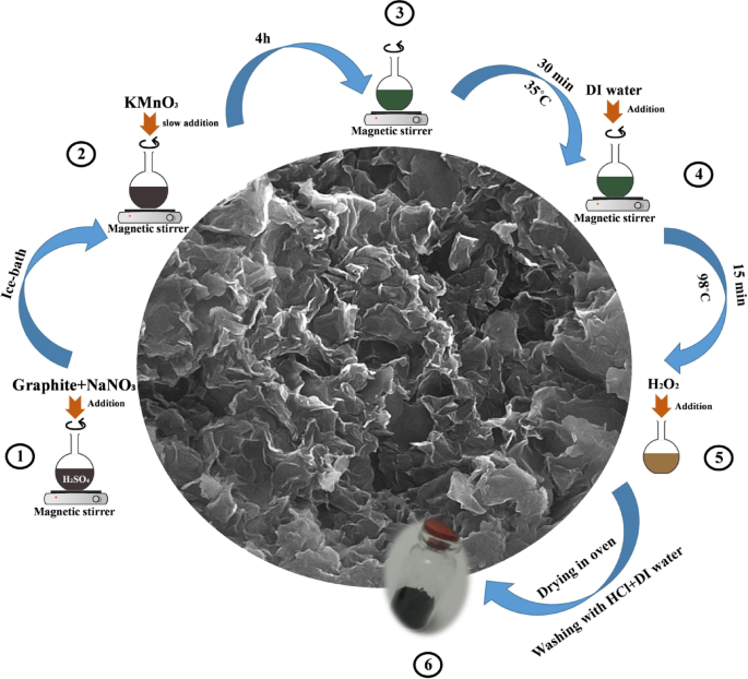
Graphite powder (> 99%, Mesh 320) was obtained from Arminano. Sulfuric acid (95–97%), KMnO4 (> 99%), and sodium nitrate (99%) were commercially available from Merck (Germany). HCl (37%) and H2O2 (30%) were purchased from Kimia Exir. All the chemicals obtained were research grade with no more purification.
The preparation of GO samples with different degrees of oxidation using Hummers’ method was conducted in the original work reported by Hummers and Offerman as follows:49 Firstly, 23 ml of sulfuric acid was poured into a round bottom flask and stirred inside an ice bath. The reaction temperature should not exceed 20 °C. In the next step, 1 g of graphite powder and 0.5 g of sodium nitrate were added to the H2SO4. After that, 3 g, 1.5 g, and 0.5 g of potassium permanganate to synthesize GO (3), GO (1.5), and GO (0.5) respectively, in separate synthesis processes were added slowly to the solution, and the obtained solution was stirred for 4 h. The product was then warmed to 35 °C while stirring for 30 min. After adding deionized water (DI), the mixture was heated in an oil bath while the overall reactant temperature was maintained at 98 °C for 15 min. The final solution was cooled down to room temperature, followed by the addition of 10 mlof hydrogen peroxide. The final synthesized products were purified with a hydrochloric acid (%37) aqueous solution (1:10, v/v) various times. The schematic diagram of the synthesis process for the preparation of GO is shown in Fig. 1.
Three samples with an ITO/GO/Al structure were fabricated through a similar process, as described below and illustrated in Fig. 2a. The RRAM devices were fabricated on a lime glass surface coated with sputtered Indium Tin Oxide (ITO). This ITO layer underwent a series of cleaning steps using DI water, Acetone, Ethanol, and Isopropanol, each followed by ultrasonic treatment for 20 min. The device was then exposed to UV light to enhance surface bonding between the bottom metal electrode and the graphene oxide. For the graphene oxide solutions, graphene oxide powder at three different oxidation levels (0.5, 1.5, and 3) was dispersed in pure DI water to a concentration of 0.5 mg/ml. The solutions were then sonicated with a microprobe for one hour at 100 Watts to ensure uniformity. We employed the spray pyrolysis deposition system described by Moazzeni et al. to deposit GO.
Schematic diagram of the synthesis process of graphene oxide (GO) with different degrees of oxidation.
thin films atop ITO19. The schematic depiction of the spray pyrolysis system is shown in Figure 2b. Finally, a 120 nm layer of aluminum was deposited atop the GO layer via RF-magnetron sputtering. This process used a shadow mask measuring 1 mm × 1 mm and operated at a pressure of 5 × 10− 3mbar at room temperature.
(a) Schematic layout of the fabricated devices (b) The schematic illustration of our spray pyrolysis system.
X-ray diffraction (XRD) characterization was performed to study the crystal structure of the prepared GO samples by an X-ray diffractometer named Bruker (model D8-ADVANCE). Figure 3 presents the XRD patterns of synthesized GO powders. According to Fig. 3, the XRD pattern of GO(3) exhibits an intense peak at 2θ = 11.45°, which is related to the (002) plane of GO, illustrating the presence of functional groups in this prepared sample50,51. This peak faced a slight shift in GO(1.5), and it occurred at 2θ = 11.6° in the XRD pattern of GO(1.5). On the other hand, this peak wholly disappeared in the GO(0.5) XRD pattern regarding the reduction of oxidation degree in GO(0.5). What’s more, a weaker peak exists in the pattern of GO(3) at 2θ = 26.7°, which is reported to be related to the (002) plane of Graphite. Reducing the oxidation degree in prepared samples relatively.
increases the intensity of this peak. (JCPDS card file No: 075-2078). As can be seen in the pattern of GO(0.5), an intense and broad peak exists at 2θ = 26.7° which reveals that this synthesized sample contains the least number of oxidation groups (the most just graphitic sheets) among all three prepared samples13,49,52. The oxidation groups consist of hydroxyl (C–OH) and carboxyl (C–O) groups, which reportedly take the resistive switching role in GO-based RRAM devices53. The size of GO sheets is generally dependent on the synthesis method. In our case, the SEM images show the formation of GO sheets ranging from a few hundred nanometers to 1 μm.
XRD patterns of synthesized GO with different degrees of oxidation.
Raman spectroscopy was utilized to examine defects and structural disorders in graphene oxide (GO) samples with varying oxidation levels. The degree of disorder was assessed by the intensity ratio between the disorder-induced D band and the Raman-allowed G band (ID/IG). The Raman spectra of the GO samples, presented in Fig. 4, indicate significant changes in oxidation levels. The spectra of GO(3), GO(1.5), and GO(0.5) exhibit intense peaks at 1350 cm−1, 1339 cm−1, and 1339 cm−1, respectively, identified as D bands. These bands signify the presence of defects in synthesized GO, such as bond-angle and bond- length disorders, vacancies, edge defects, etc. Additionally, the spectra display another intense peak at 1592 cm−1, 1588 cm−1, and 1570 cm−1 for GO(3), GO(1.5), and GO(0.5), respectively, corresponding to the G band. According to Fig. 4, the G band shifts to a higher wavenumber (from 1570 to 1592 cm−1) due to graphite oxidation, and the D band intensity increases, indicating the formation of defects and disorders, including in-plane hetero-atoms, grain boundaries, aliphatic chains, etc. The increase in the D-band intensity ratio corresponds to enhanced structural disorder, consistent with the higher trap density responsible for the observed I–V nonlinearity and switching variability. Furthermore, two other important, albeit weak and broad, peaks in the Raman spectra of the GO samples are the 2D and D + G bands. The 2D peak appears at 2680 cm−1, 2662 cm−1, and 2667 cm−1 in the spectra of GO(3), GO(1.5), and GO(0.5), respectively, while the D + G band appears at 2923 cm−1, 2925 cm−1, and 2927 cm−1. As the Raman spectra indicate, the intensity of the 2D bands diminishes with an increase in the oxidation degree of the GO samples, attributed to deformation in the stacking order along the c-axis. Since the 2D band is susceptible to this stacking order, the oxidation reaction disrupts the stacking order in graphite, reducing the intensity and sharpness of the 2D band. Conversely, the intensity of the D + G bands increases with the oxidation degree of the GO samples, showing a trend opposite to that of the 2D band54,55,56.
Raman spectra of the GO with different degrees of oxidation.
The ID/IG ratios were extracted from the fitted Raman spectra (Fig. 5) and are summarized in Table 1. The results show that the ID/IG ratio increases from GO(0.5) to GO(1.5), confirming that higher KMnO₄ concentration enhances the density of defects and oxygen functional groups. A slight reduction at GO(3) is attributed to over-oxidation and partial disruption of the sp² domains, which reduces the relative intensity of the D-band. This non-monotonic behavior is consistent with previous reports on graphene oxide and indicates that excessive oxidation can lead to partial structural degradation.
Raman Intensity comparison of D band G bands of synthesis samples.
Fourier transform infrared (FTIR) spectroscopy was employed to identify and analyze the surface functional groups of GO samples with various oxidation levels. The FTIR spectra of the GO samples with different oxidation levels are shown in Fig. 6. The broad absorption band around 3400 cm⁻¹ corresponds to hydroxyl (O–H) stretching vibrations, while the peaks near 1720 cm⁻¹ and 1220 cm⁻¹ represent carbonyl (C=O) and epoxy (C–O–C), respectively. The 1050 cm⁻¹ peak is assigned to C–O stretching. A clear trend is observed where GO(3) exhibits the most intense oxygen-related bands, GO(1.5) shows intermediate intensities, and GO(0.5) presents the weakest features57,58. Interestingly, in some cases a partially oxidized sample (e.g., GO(1.5)) may display relatively stronger absorption for certain bands compared to the over-oxidized GO(3), which can be attributed to structural disorder, transformation of labile oxygen groups, or scattering effects at higher oxidant concentrations. This deviation is commonly associated with over-oxidation, where excessive KMnO₄ disrupts the sp² network and removes unstable oxygen functionalities instead of creating new ones. These results confirm that oxygen-containing functional groups directly correlate with KMnO₄ concentration and critically govern the resistive switching behavior of the devices59. The progressive increase in the intensity of O–H, C6=O, and C–O stretching modes with KMnO₄ concentration generally reflects the higher density of oxygen functional groups, which play a crucial role in charge trapping and conduction path modulation in RRAM devices.
FTIR test results of synthesized GO with different degrees of oxidation.
Surface morphologyThe morphology of the graphene oxide (GO) samples in this study was examined using Field Emission Scanning Electron Microscopy (FESEM, model: MIRA3 TESCAN-XMU). FE-SEM images of the deposited GO samples (0.5, 1.5, and 3) and their corresponding higher magnifications are presented in Figs. 7a, c, e and Fig. 7b, d, f , respectively. As graphite oxidizes, its layers start to separate. These exfoliated GO layers have varying numbers of stacked layers, depending on the degree of oxidation. Higher oxidation levels increase the distance between GO layers, leading to further separation. For example, the FE- SEM image of the lower oxidation level GO (0.5) reveals numerous stacked GO sheets. The red arrow in Fig. 7b points to a stacked structure of GO sheets. On the other hand, with increased oxidation levels achieved by using a more significant amount of the oxidizing agent KMnO4, the GO layers exhibit more exfoliation and higher degrees of oxidation compared to those with lower oxidation levels56. Blue arrows indicate some of these exfoliated GO layers in Fig. 7f. The higher exfoliation and reduced stacking of GO sheets at increased KMnO₄ concentrations arise from the incorporation of oxygen functional groups (O–H, C=O, C–O). These groups enlarge the interlayer spacing and disrupt van der Waals interactions, thereby modifying the film morphology consistently with the oxidation degree.
SEM images of the (a, b) GO(0.5) sheets (c, d) GO(1.5) sheets (e, f) GO(3) sheets at low and high magnification.
Atomic Force Microscopy (AFM) was employed to examine the surface topography of the deposited graphene oxide (GO) solutions. The forward scan analysis was conducted using a 200 nm tip over a 50 μm × 50 μm area. Figure 8a–c displays the AFM results for all three samples, obtained using the NanoSurf Naio AFM tool. Consequently, the AFM findings demonstrate the uniform deposition of GO solutions across all samples.
The AFM image of (a) GO(0.5) (b) GO(1.5) and (c) GO(3).
AFM quantitative analysis (Table 2) confirms that the GO(1.5) film exhibits the highest RMS roughness ( 123 nm), while the GO(3) film becomes slightly smoother ( 114 nm) with increased oxidation. The local peak-to-valley amplitudes decrease from 151 nm to 97 nm, reflecting enhanced uniformity at higher oxidation levels. These morphological trends directly influence the contact behavior and switching performance of the RRAM devices.
The electrical measurements of the fabricated Resistive Random Access Memory (RRAM) devices were recorded using a Keithley 2450 source measurement unit under ambient con- ditions. The electrical characteristics, including resistive switching behavior, were studied using a triangular DC voltage sweep. For endurance and retention measurements, the I–V characteristics were repeatedly recorded under a triangular DC sweep using a Keithley 2450 source-measurement unit. A compliance current of 10 mA was applied during the SET process to prevent hard breakdown. The Ion/Ioff ratio was extracted at a read voltage of 1 V for each cycle. Retention measurements were performed by monitoring the HRS and LRS currents at 1 V over time without further biasing. This procedure ensures that endurance variability and retention stability can be consistently compared across devices. A positive bias was applied to the top electrode (Al), while the bottom electrode (ITO) was grounded. Figure 9a displays the semi-logarithmic I–V characteristics of RRAMs with GO(3) as the active layer, showing the device initially in the HRS. The measurement process began with a voltage sweep from 0 V to 3.5 V until the electrical current reached the compliance current (CC). In this manner, a 10 mA compliance current was set to prevent the device breakdown. So, the electrical current of the memory showed a gradual increase from 0 V to 1.1 V, followed by a steeper increase from 1.2 V to 2.8 V, where it reached the compliance current (SET Process). The initial resistance at 1 V (HRS) was 55 KΩ, dropping to 280 Ω at 2.8 V, indicating resistive switching. While sweeping the voltage back from 3.5 V to 0 V, the device remained in the LRS. The HRS resistance to LRS resistance ratio (RHRS/RLRS) at 1 V was approximately 120. Finally, the voltage was swept from 0 to − 3 V to reset the device to HRS (RESET process). The slope of the I–V curve showed a resistance increase beyond − 2.1 V. The second cycle of write/erase is illustrated in red, showing established conductive paths in the GO layer, with LRS current values similar to the first cycle, resulting in an ILRS/IHRS ratio of around 20 at 1 V. At low bias, the LRS exhibits near-ohmic behavior consistent with carbon-rich (sp²-dominated) conductive paths, whereas departures at higher fields reflect trap-assisted/SCLC transport; consequently, the LRS shows metallic-like thermal response without invoking a purely metallic filament.
Figure 9b presents the semi-logarithmic I–V characteristics of the GO (1.5) RRAM. The inset shows the device’s schematic layout. The initial state was HRS, and upon sweeping from 0 to 3 V (SET process), the device transitioned to LRS at 3.4 mA current without overshooting. The overshoot phenomenon in SET operations can negatively affect cycle-to- cycle variation in RRAMs60. Unlike the GO (3) device, current compliance was not necessary due to the gradual current rise. The memory window (ILRS/IHRS) at 1 V was 3.5, smaller than that of the GO (3) RRAM. The RESET process did not show abrupt conduction changes, but the resistance reduction was evident during the sweeping back. Interestingly,
the second switching cycle showed no significant difference from the first, indicating the GO(1.5) RRAM’s bipolar, forming-free, compliance-current-free, and overshoot-suppressed switching behavior, desirable for brain-inspired computing applications in RRAMs26,48,61.
Figure 9c displays the I–V characteristics of the GO(0.5) device. With a compliance current of 10 mA, the device reached the compliance current at 1.5 V, faster than the other samples. The ILRS/IHRS ratio at 1 V was as low as 1.1, and the electrical resistance in the pristine state was significantly lower than that of the GO(1.5) and GO(3) devices. The RE- SET process showed no significant resistance reduction. Overall, the I–V analysis highlights a clear relationship between the oxidation level of GO and various electrical parameters of the RRAM devices, such as the forming process, transition type, and Ion/Ioff. Figure 9d illustrates the Ion/Ioff ratio for the first two SET/RESET cycles of the three RRAM devices. Notably, a reduction in the oxidation level has decreased the Ion/Ioff ratio. Compared to the GO(3) device, the GO(1.5) RRAM exhibits a higher HRS current and a lower LRS current, resulting in a lower Ion/Ioff ratio. Conversely, the GO(0.5) device shows higher currents in both HRS and LRS. Additionally, it is observed that the difference between the first and second cycles is minimal in the GO(1.5) and GO(0.5) RRAMs, in contrast to the GO(3) device. In this work, forming-free denotes the absence of a distinct high-voltage activation step outside the normal operating window and the absence of an abrupt, irreversible breakdown prior to regular cycling. For GO(1.5), the first and subsequent I–V cycles overlap within the same bias range and no compliance is required, with overshoot suppressed—consistent with forming-free operation (Fig. 9b). For GO(3), a slight current increase during the first up-sweep is observed; however, this transition is gradual, occurs within the regular sweep window, and is fully reversible in subsequent cycles, indicating soft electro-conditioning (trap filling/redistribution of oxygen-related groups) rather than classical electroforming.
To evaluate the retention characteristics of our graphene oxide (GO) RRAMs, the currents in the HRS and LRS were recorded separately at a 1 V reading voltage. As depicted in Figure. 10a, b, the GO(1.5) and GO(3) RRAMs successfully maintained retention for up to 6 × 10³.
seconds at room temperature. These results indicate that the GO(3) and GO(1.5) RRAMs are nonvolatile, sustaining the memory window with only slight narrowing. However, the retention characteristics of the GO (0.5)-based memory were not as stable. As shown in Fig. 10c, the LRS current of the GO(0.5)-based memory drops after just 20 s and fails to maintain the LRS state. Consequently, due to the instability and negligible Ion/Ioff, in the GO(0.5) device, our subsequent characterizations, and discussions will focus solely on the GO(1.5) and GO(3)-based RRAMs. The systematic correlation between oxidation-dependent FTIR, Raman, and XRD results and the I–V characteristics strongly supports that the resistive switching in GO films is governed by defect-mediated conduction through oxygen functional groups. The weak temperature dependence of the LRS current further supports metallic-like conduction through stable conductive filaments. Previous investigations on graphene oxide–based RRAMs have similarly reported that the ON-state resistance follows a metallic trend with a low temperature coefficient32. Consistent with general observations in ReRAM systems, the ON state typically exhibits ohmic conduction with minimal thermal activation62. Furthermore, thermal modeling of conductive filaments suggests that the internal temperature rise is highly localized, resulting in a low effective temperature coefficient of resistance across the filament cross-section63.
The semi-logarithmic I–V characteristics of the (a) GO(3), (b) GO(1.5), and (c) GO(0.5) RRAMs in the first and second RS cycles. (d) the Ion/Ioff ratio of three devices in the 1st and 2nd SET/RESET cycle.
The retention characteristics of (a) GO(3) (b) GO(1.5) (c) GO(0.5) RRAMs at 1 V reading voltage.
Figure 11a, b displays the endurance characteristics of the GO(1.5) and GO(3) RRAMs by showing the LRS and HRS currents at a 1 V reading voltage. The characterization swept the DC bias from 3 V to − 3 V. The endurance results for this device demonstrate stable SET and RESET across the first 50 cycles with negligible fluctuation (the inset shows the I–V diagram of the endurance characterization for the devices). It is evident from the endurance figure that GO(3) exhibits higher cycle-to-cycle (C2C) variation compared to the GO(1.5) device. To illustrate and analyze the C2C variation, the cumulative distribution of HRS and LRS currents for both devices is shown in Fig. 11c. This figure demonstrates a wider variation for the GO(3) device in HRS and LRS. Furthermore, the variation in HRS current is more pronounced than in LRS for both RRAMs, which is attributed to the localized conduction paths in LRS. In contrast, the conduction mechanism in HRS is bulk conduction dependent on individual and non-uniform trap sites37,64. Fig. 11d compares variance in both samples.
To study the conduction mechanism in the GO-based RRAMs, the I–V relationship was plotted on a double logarithmic scale. As depicted in Fig. 12a, a nearly linear relation- ship with a slope of 1.17 exists between current and voltage at low voltages (< 1 V ) during the positive sweep. The subsequent current shows a dependence on voltage with a slope of 2.68, indicating that the switching mechanism in the high voltage regime is governed by Space Charge Limited Current (SCLC)37,65. This rapid increase in current due to SCLC suggests the induction of numerous non-intrinsic carriers within the dielectric layer, followed by trap filling with electrons injected via the top electrode66,67. In the reverse sweep, the LRS current maintains conduction with a slope of 1.27, reinforcing the notion of conductive path formation along the GO layer after switching. Significantly, the non-ohmic conduction relationship in HRS contradicts this device’s idea of metallic filament formation during resistive switching. Based on our discussions in the introduction section about resistive switching mechanisms, the dominant mechanism is not limited to metallic filament formation or in- terface modulation. This is because either of these mechanisms would result in an ohmic.
The endurance characteristics of (a) GO(1.5) (b) GO(3) RRAMs (The inset de- picts the cyclic I–V diagram of fabricated RRAMs) (c) Cumulative distribution probabilities of HRS and LRS obtained from the endurance test (d) The variance of HRS and LRS en- durance’s data of GO(1.5) and GO(3) RRAMs.
relationship during the LRS. Such a relationship would be due to the forming of a metallic filament within the Graphene Oxide or an interface-modulated layer, respectively. Therefore, we propose that the significant mechanism governing resistive switching is the formation of conductive paths along the GO layer due to the movement of functional groups energized by electric pulses.
Figure 12b shows that the RRAM still does not exhibit a completely ohmic behavior during the LRS and RESET process in the negative sweep. Here, the slope reduction in LRS from 1.12 to 0.91 suggests the rupture of conductive paths due to carrier relocation on the graphene sheets. Figure 12c presents the double logarithmic I–V diagram of the GO(3) RRAM. In the positive sweep, the device’s current follows an I–V relationship with a slope of 1.31 in the low voltage region (< 0.7 V ). Then, the slope increases in two subsequent regions with slopes of 2.53 and 6.61, corresponding to the unfilled traps and trap-filled regions, respectively, indicating SCLC as the governing conduction mechanism during the SET process61,66. In LRS, the current again follows a non-ohmic relationship, implying the formation of a non-metallic conductive path within the GO film. Figure 12d depicts the negative sweep, where the current-voltage relationship remains non-ohmic, decreasing with a slope of 0.31. The conduction mechanism during the RESET process resembles the SET process, with SCLC followed by a non-ohmic relationship. Notably, there is a significant difference between the slopes in similar regions of the SET transition in GO(3) and GO(1.5) devices. The larger slope in GO(3) can be attributed to the higher oxidation level, which provides a larger number of non-intrinsic carriers under electric field force. Conversely, the GO(1.5) device exhibits a smaller slope during the SET transition, correlating with its lower oxidation level. This trend is also evident in the positive LRS region, where the GO(3) device exhibits a larger slope than the GO(1.5) device.
The I–V double logarithmic characteristics of GO(1.5)-based RRAM in (a) positive sweep (SET) (b) negative sweep (RESET), GO(3)-based RRAM in (c) positive sweep (SET) (d) negative sweep (RESET)..
As discussed in the introduction, three central mechanisms have been proposed to account for resistive switching in GO resistive random-access memories (RRAMs). After analyzing the oxidation levels in fabricated GO RRAMs, we suggest the drift of oxygen-based functional groups (C–O, C–OH) as the dominant mechanism in our devices. During the SET process, applying an electrical field along the GO layer provides sufficient energy for the detachment of negatively charged oxygen groups. These detached oxygen ions exhibit deficient migration barrier energy, enabling them to drift toward the top electrode under the electric field. Con- sequently, the insulating sp3 bonding is transformed into conductive sp2 bonding, forming a conductive path along the GO layer. This underscores the critical role of oxygen groups in the SET process dynamics11,37. Ki Hong et al. demonstrate that the distribution of oxygen functional groups along the GO film significantly changes after applying an electric field. In the same study, in-depth X-ray photoelectron spectroscopy (XPS) characterization of the GO film confirms the movement of oxygen in LRS and HRS. In our characterization, we also observed that GO(1.5) RRAM with a low oxidation level exhibited lower conductivity in the LRS state than GO(3) RRAM, even though they displayed similar conductivity in the HRS state. This theory can explain why the device with a lower oxygen level does not require a forming process, as a thick and robust conductive path cannot be formed due to the lack of sufficient sp2 regions. Instead, several thin conductive paths are likely formed, which will be ruptured entirely during the RESET process. Another piece of evidence supporting this mechanism is the nonlinear I–V relationship during the positive LRS. If the other mecha- nisms were dominant, the LRS current would follow a linear (ohmic-metallic) relationship, as the filaments in the two mechanisms have metallic properties. However, our devices exhibit a non-ohmic relationship influenced by the oxidation level or the concentration of oxygen groups on GO sheets. Moreover, applying an electric field in the reverse direction during the RESET process energizes the oxygen ions to move back to their initial positions and re- bind with the graphene sheets. The sp2 bonding transitions back to insulating sp3 bonding.
through these movements. Furthermore, in the RESET process of the GO(3) device, we can observe a transition region with negative resistance in its I–V characteristic. At the same time, it does not exist in the GO(1.5) device. We attribute this phenomenon to multiple conductive paths in GO(1.5) rather than a single conductive path in the GO(3) device. Con- sequently, in the GO(1.5) device, applying a negative bias initiates the rupture process of several conductive paths, which may not necessarily co-occur. Hence, the RESET transition is more gradual. On the other hand, in the GO(3) device, the application of a negative voltage disrupts the only conductive path, resulting in a period of negative resistivity in the device, as further voltage increase at that moment leads to further rupture of the conductive path. Figure 13a, b depicts the difference between the switching mechanism in GO(1.5) and GO(3). In summary, our characterization results reveal that the resistive switching behavior of GO-based RRAMs is primarily governed by the migration of oxygen-containing functional groups. By correlating structural (XRD), spectroscopic (FTIR, Raman), and electrical analyses, it is demonstrated that the KMnO₄ concentration determines the density and distribution of these functionalities, thereby modulating the I–V characteristics through interface adjustment and filament dynamics. The variation of the ON/OFF ratio among the GO devices can be understood in terms of the oxidation-dependent density of oxygen functional groups. Higher KMnO₄ concentrations introduce more oxygenated groups and structural disorder, which increase the number of available trap sites and strongly modulate the HRS conductivity. In contrast, the LRS conductivity is mainly governed by the stability of conductive paths and remains relatively less sensitive to oxidation degree. This imbalance explains why the Ion/Ioff ratio increases for higher oxidation levels, but also why greater cycle-to-cycle variation is observed in GO(3). The correlation of these electrical findings with FTIR and Raman analyses ensures consistency between structural characterization and conductometric measurements.
We demonstrate the ability to control GO-based RRAM’s performance metrics by varying the GO layer’s oxidation level. In this context, we could alter the Ion/Ioff ratio and diminish the significance of the forming process in these devices. Additionally, our results show reduced cycle-to-cycle variation in devices with lower oxidation. These findings highlight the critical role of defect engineering in RRAM technology, especially in carbon-based devices, to achieve forming-free and analog resistive switching. Furthermore, our results have enabled us to propose a comprehensive understanding of the origin of resistive switching in GO-based RRAMs. Our proposed mechanism focuses on the movement of oxygen-based functional groups as the key factor responsible for resistive switching in GO-based RRAMs.
The schematic illustration of switching mechanism in (a) GO(3) (b) GO(1.5) based RRAM.
The datasets used and/or analysed during the current study available from the corresponding author on reasonable request.
Zhang, C., Li, Y., Ma, C. & Zhang, Q. Recent progress of organic-inorganic hybrid perovskites in RRAM, artificial synapse, and logic operation. Small Sci. 2, 2100086 (2022).
Article PubMed Google Scholar
Johari, S. et al. CMOS-memristor hybrid design of a neuromorphic crossbar array with integrated inference and training. in 2024 IEEE 67th International Midwest Symposium on Circuits and Systems (MWSCAS) 442–446 (2024).
Das, S. & Mao, E. The global energy footprint of information and communication tech- nology electronics in connected Internet-of-Things devices. Sustainable Energy Grids Networks. 24, 100408 (2020).
Article Google Scholar
Burr, G. W. et al. Others neuromorphic computing using non- volatile memory. Adv. Physics: X. 2, 89–124 (2017).
ADS Google Scholar
Upadhyay, N. K. et al. Emerging memory devices for neuromorphic computing. Adv. Mater. Technol. 4, 1800589 (2019).
Article Google Scholar
Varshika, M. L. et al. Design of a Tunable astrocyte neu-romorphic circuitry with adaptable fault tolerance. in 2023 IEEE 66th International Midwest Symposium on Circuits and Systems (MWSCAS) 904–908 (2023).
Xi, Y. et al. In-memory learning with analog resistive switching memory: A review and perspective. Proc. IEEE. 109, 14–42 (2020).
Article ADS Google Scholar
Kwon, K. C., Baek, J. H., Hong, K., Kim, S. Y. & Jang, H. W. Memristive devices based on two-dimensional transition metal chalcogenides for neuromorphic computing. Nano-Micro Lett. 14, 58 (2022).
Article ADS Google Scholar
Koveshnikov, S. et al. Multiple resistive switching mechanisms in graphene oxide- based resistive memory devices. Nanomaterials 12, 3626 (2022).
Article PubMed PubMed Central Google Scholar
Hui, F. et al. Graphene and related materials for resistive random access memories. Adv. Elec- Tronic Mater. 3, 1600195 (2017).
Article Google Scholar
Qi, M. et al. Uniform multilevel switching of graphene oxide-based RRAM achieved by embedding with gold nanoparticles for image pattern recognition. Appl. Phys. Lett. 116, 163503 (2020).
Article ADS Google Scholar
Nagareddy, V. K. et al. Multilevel ultrafast flexible nanoscale nonvolatile hybrid graphene oxide– titanium oxide memories. Acs Nano. 11, 3010–3021 (2017).
Article PubMed Google Scholar
Krishnamoorthy, K., Veerapandian, M., Yun, K. & Kim, S. J. The chemical and struc- tural analysis of graphene oxide with different degrees of oxidation. Carbon 53, 38–49 (2013).
Article Google Scholar
Romero, F. J. et al. Resistive switching in graphene oxide. Front. Mater. 7, 17 (2020).
Article ADS Google Scholar
Madvar, H. R., Moayedi, M. & Kordrostami, Z. Impact of reduced-graphene-oxide func- tionalization of flower-like zinc-oxide nanostructures on sensing performance of resistive ethanol gas sensor. Thin Solid Films. 804, 140498 (2024).
Article ADS Google Scholar
Jeong, H. Y. et al. Others graphene oxide thin films for flexible nonvolatile memory applications. Nano Lett. 10, 4381–4386 (2010).
Article ADS PubMed Google Scholar
Saini, P. et al. Probing the mechanism for bipolar resistive switching in annealed graphene oxide thin films. ACS Appl. Mater. Interfaces. 10, 6521–6530 (2018).
Article PubMed Google Scholar
Moazzeni, A. & Hamedi, S. Fabrication of non-volatile resistive switching memory based on graphene oxide and PEDOT: PSS mixture. in 2020 28th Iranian Conference on Electrical Engineering (ICEE) 1–4 (2020).
Moazzeni, A., Riyahi Madvar, H., Hamedi, S. & Kordrostami, Z. Fabrication of graphene Oxide-Based resistive switching memory by the spray pyrolysis technique for Neuro- morphic computing. ACS Appl. Nano Mater. 6, 2236–2248 (2023).
Article Google Scholar
Udowo, V. M., Yan, M., Liu, F., Okafor, P. C. & Louis, H. Computational and experi- mental study of the electronic and chemical changes of graphene oxide-doped PEDOT in aqueous solution. J. Mater. Sci. 58, 13605–13620 (2023).
Article ADS Google Scholar
Shi, K. et al. Complementary resistive switching observed in graphene oxide-based memory device. IEEE Electron Device Lett. 39, 488–491 (2018).
Article ADS Google Scholar
Moazzeni, A. & Kordrostami, Z. Others switching characteristic of fabricated nonvolatile bipolar resistive switching memory (ReRAM) using PEDOT: PSS/GO. Solid State Electron. 188, 108208 (2022).
Article Google Scholar
Zhao, X. et al. Photocatalytic reduction of graphene oxide–TiO2 nanocomposites for improving resistive-switching memory behaviors. Small 14, 1801325 (2018).
Article Google Scholar
Ansari, H. R. et al. Flexible/wearable resistive gas sensors based on 2D materials. J. Mater. Chem. C (2023).
Shi, T. et al. A review of resistive switching de- vices: performance improvement, characterization, and applications. Small Struct. 2, 2000109 (2021).
Article Google Scholar
Kim, H., Mahmoodi, M., Nili, H. & Strukov, D. B. 4K-memristor analog-grade passive crossbar circuit. Nat. Commun. 12, 5198 (2021).
Article ADS PubMed PubMed Central Google Scholar
Kang, H. et al. Two-and three- terminal HfO2-based multilevel resistive memories for neuromorphic analog synaptic elements. Neuromorphic Comput. Eng. 1, 021001 (2021).
Article Google Scholar
Xu, C., Dong, X., P Jouppi, N. & Xie, Y. Design implications of memristor-based RRAM cross-point structures. Des. Autom. Test. Europe. 2011, 1–6 (2011).
Google Scholar
Qi, M., Guo, C. & Zeng, M. Oxygen vacancy kinetics mechanism of the negative forming-free process and multilevel resistance based on hafnium oxide RRAM. J. Nanomater. 2019, 6724018 (2019).
Article Google Scholar
Chen, S. & Valov, I. Design of materials configuration for optimizing redox-based resistive switching memories. Adv. Mater. 34, 2105022 (2022).
Article Google Scholar
Ricci, S., Mannocci, P., Farronato, M., Hashemkhani, S. & Ielmini, D. Forming-Free resistive switching memory crosspoint arrays for In-Memory machine learning. Ad- Vanced Intell. Syst. 4, 2200053 (2022).
Article Google Scholar
Zhuge, F. et al. Mechanism of nonvolatile resistive switching in graphene oxide thin films. Carbon 49, 3796–3802 (2011).
Article Google Scholar
Jetty, P., Sahu, D. P. & Jammalamadaka, S. Analog resistive switching in reduced graphene oxide and chitosan-based bio-resistive random access memory device for neu- romorphic computing applications. Phys. Status Solidi (RRL)–Rapid Res. Lett. 16, 2100465 (2022).
Article ADS Google Scholar
Qi, M. et al. Oxidized carbon quantum dot–graphene oxide nanocomposites for improving data retention of resistive switching memory. J. Mater. Chem. C. 6, 2026–2033 (2018).
Article Google Scholar
Zhou, S. & Bongiorno, A. Origin of the chemical and kinetic stability of graphene oxide. Sci. Rep. 3, 2484 (2013).
Article ADS PubMed PubMed Central Google Scholar
Romero, F. J. et al. Laser-Fabricated reduced graphene oxide memristors. Nanomaterials 9, 897 (2019).
Article PubMed PubMed Central Google Scholar
Rodriguez, N. et al. Resistive switching and charge Trans- Port in Laser-Fabricated graphene oxide memristors: A time series and quantum point contact modeling approach. Nanomaterials 12, 3734 (2019).
ADS Google Scholar
Banerjee, W., Liu, Q. & Hwang, H. Engineering of defects in resistive random access memory devices. J. Appl. Phys. 127, 051101 (2020).
Article ADS Google Scholar
Tutuncuoglu, G. & Mannodi-Kanakkithodi, A. Role of defects in resistive switching dy- Namics of memristors. MRS Commun. 12, 531–542 (2022).
Article ADS Google Scholar
Farahmandpour, M., Ansari, H. R. & Kordrostami, Z. Flexible enzyme-free gate engineered Bio-FET glucose sensor based on nickel-tungstate microcrystals. IEEE Sens. J. 24(7), 9308–9316 (2024).
Article ADS Google Scholar
Yang, Y., Choi, S. & Lu, W. Oxide heterostructure resistive memory. Nano Lett. 13, 2908–2915 (2013).
Article ADS PubMed Google Scholar
Li, Y. et al. Others tuning the resistive switching in tantalum oxide-based memristors by annealing. AIP Adv. 10, 065112 (2020).
Article ADS Google Scholar
Jiang, H. & Stewart, D. A. Using dopants to tune oxygen vacancy formation in transition metal oxide resistive memory. ACS Appl. Mater. Interfaces. 9, 16296–16304 (2017).
Article PubMed Google Scholar
Simanjuntak, F. M., Ohno, T., Chandrasekaran, S., Tseng, T. Y. & Samukawa, S. Neu- tral oxygen irradiation enhanced forming-less ZnO-based transparent analog memristor devices for neuromorphic computing applications. Nanotechnology 31, 26LT01 (2020).
Article PubMed Google Scholar
Saleem, A. et al. Transformation of digital to analog switching in TaOx-based memris- Tor device for neuromorphic applications. Appl. Phys. Lett. 118, 112103 (2021).
Article ADS Google Scholar
Sarkar, B., Lee, B. & Misra, V. Understanding the gradual reset in Pt/Al2O3/Ni RRAM for synaptic applications. Semicond. Sci. Technol. 30, 105014 (2015).
Article ADS Google Scholar
Kim, H. J. et al. Digital versus analog resistive switching depending on the thickness of nickel oxide nanoparticle assembly. RSC Adv. 3, 20978–20983 (2013).
Article ADS Google Scholar
Kim, S. et al. 4-bit multilevel operation in overshoot suppressed Al2O3/TiOx resistive Random-Access memory crossbar array. Adv. Intell. Syst. 4, 2100273 (2022).
Article Google Scholar
Chen, C. et al. Effective synthesis of highly oxidized graphene oxide that enables Wafer-scale nanopatterning: preformed acidic oxidizing medium approach. Sci. Rep. 7, 1–10 (2017).
Google Scholar
Yasin, G. et al. Exploring the nickel–graphene nanocomposite coatings for superior corro- Sion resistance: manipulating the effect of deposition current density on its morphology, mechanical properties, and erosion–corrosion performance. Adv. Eng. Ma- Terials. 20, 1701166 (2018).
Article Google Scholar
Soomro, S. A., Gul, I. H., Naseer, H., Marwat, S. & Mujahid, M. Improved performance of CuFe2O4/rGO nanohybrid as an anode material for lithium-ion batteries prepared via facile one-step method. Curr. Nanosci. 15, 420–429 (2019).
Article ADS Google Scholar
Wang, J. T., Chen, C., Li, H. D., Mizuseki, H. & Kawazoe, Y. Three-dimensional carbon allotropes comprising phenyl rings and acetylenic chains in sp + sp2 hybrid networks. Sci. Rep. 6, 24665 (2016).
Article ADS PubMed PubMed Central Google Scholar
Hong, S. K., Kim, J. E., Kim, S. O. & Cho, B. J. Analysis on switching mechanism of graphene oxide resistive memory device. J. Appl. Phys. 110, 044506 (2011).
Article ADS Google Scholar
Perumbilavil, S., Sankar, P., Rose, T. P. & Philip, R. White light Z-scan measurements of ultrafast optical nonlinearity in reduced graphene oxide nanosheets in the 400–700 Nm region. Appl. Phys. Lett. 107, 051104 (2015).
Article ADS Google Scholar
Hafiz, S. M. et al. Others A practical carbon dioxide gas sensor using room-temperature hydrogen plasma reduced graphene oxide. Sens. Actuators B. 193, 692–700 (2014).
Article Google Scholar
Pareek, S. et al. Tunable degree of oxidation in graphene oxide: cost effective synthesis, characterization and process optimization. Mater. Res. Express. 6, 085625 (2019).
Article ADS Google Scholar
Mathioudakis, G. N., Visvini, G. A., Sygellou, L. & Voyiatzis, G. A. Comparative In-Depth investigation of benchmark graphene oxides in the perspective of their integration into industrial production processes. Nanomaterials 15, 1–15 (2025).
Article Google Scholar
Lyn, F. H., Peng, T. C., Ruzniza, M. Z. & Hanani, Z. A. N. Effect of oxidation degrees of graphene oxide (GO) on the structure and physical properties of chitosan / GO composite films. Food Packag Shelf Life. 21, 100373 (2019).
Article Google Scholar
Ali, B., Xu, H., Sang, R. T., Litvinyuk, V. & Rybachuk, M. I. Optimised diamond to graphite conversion via a metastable sp 1 -bonded carbon chain formation under an ultra-short femtosecond (30 fs) laser irradiation. Carbon 204, 575–586 (2023).
Article Google Scholar
Fan, Y. S. et al. Direct evidence of the overshoot suppression in Ta2O5-based resistive switching memory with an integrated access resistor. IEEE Electron Device Lett. 36, 1027–1029 (2015).
Article ADS Google Scholar
Li, Y., Wang, Z., Midya, R., Xia, Q. & Yang, J. J. Review of memristor devices in neuromorphic computing: materials sciences and device challenges. J. Phys. D. 51, 503002 (2018).
Article ADS Google Scholar
Wang, C. et al. Conduction mechanisms, dynamics and stability in rerams. Microelectron. Eng. 187–188, 121–133 (2018).
Google Scholar
Aguilera-Pedregosa, C. et al. Thermal characterization of conductive filaments in unipolar resistive memories (2023).
Lee, M. J. et al. Others A fast, high-endurance and scalable non-volatile memory device made from asymmetric Ta2O5- x/TaO2- x bilayer structures. Nat. Mater. 10, 625–630 (2011).
Article ADS PubMed Google Scholar
Lim, E. W. & Ismail, R. Conduction mechanism of Valence change resistive switching memory: A survey. Electronics 4, 586–613 (2015).
Article Google Scholar
Zhang, X. G. & Pantelides, S. T. Theory of space charge limited currents. Phys. Rev. Lett. 108, 266602 (2012).
Article ADS PubMed Google Scholar
Zhang, P. et al. Space–charge limited current in nanodiodes: Ballistic, collisional, and dynamical effects. J. Appl. Phys. 129, 100902 (2021).
Article ADS Google Scholar
Download references
Department of Electrical and Electronics Engineering, Shiraz University of Technology, Shiraz, Iran
Alireza Moazzeni, Hadi Riyahi Madvar, Samaneh Hamedi & Zoheir Kordrostami
Department of Electronics and Computer Engineering, Wayne State University, Detroit, MI, USA
Alireza Moazzeni
Research Center for Design and Fabrication of Advanced Electronic Devices, Shiraz, Iran
Hadi Riyahi Madvar & Zoheir Kordrostami
PubMed Google Scholar
PubMed Google Scholar
PubMed Google Scholar
PubMed Google Scholar
A.M., and H.R.M. wrote the revised manuscript and S.H. and Z.K. edited the manuscript.
Correspondence to Samaneh Hamedi.
The authors declare no competing interests.
Springer Nature remains neutral with regard to jurisdictional claims in published maps and institutional affiliations.
Open Access This article is licensed under a Creative Commons Attribution-NonCommercial-NoDerivatives 4.0 International License, which permits any non-commercial use, sharing, distribution and reproduction in any medium or format, as long as you give appropriate credit to the original author(s) and the source, provide a link to the Creative Commons licence, and indicate if you modified the licensed material. You do not have permission under this licence to share adapted material derived from this article or parts of it. The images or other third party material in this article are included in the article’s Creative Commons licence, unless indicated otherwise in a credit line to the material. If material is not included in the article’s Creative Commons licence and your intended use is not permitted by statutory regulation or exceeds the permitted use, you will need to obtain permission directly from the copyright holder. To view a copy of this licence, visit http://creativecommons.org/licenses/by-nc-nd/4.0/.
Reprints and permissions
Moazzeni, A., Riyahi Madvar, H., Hamedi, S. et al. Controlled oxidation levels in graphene oxide to achieve forming-free and analog resistive switching in RRAM. Sci Rep 15, 45074 (2025). https://doi.org/10.1038/s41598-025-32232-2
Download citation
Received:
Accepted:
Published:
Version of record:
DOI: https://doi.org/10.1038/s41598-025-32232-2
Anyone you share the following link with will be able to read this content:
Sorry, a shareable link is not currently available for this article.
Provided by the Springer Nature SharedIt content-sharing initiative
Advertisement
Scientific Reports (Sci Rep)
ISSN 2045-2322 (online)
© 2026 Springer Nature Limited
Sign up for the Nature Briefing newsletter — what matters in science, free to your inbox daily.